JLCParts Falling Down To Ashes

About 2 years ago, I started a small and dirty project – a new catalog for the search engine for the components that JLC PCB provides for their assembly service. The motivation was really personal — I liked the dirt-cheap assembly service, but finding the suitable components for my projects was really painful. So I created JLCParts – a browser-only alternative component catalog that doesn’t need any sophisticated backend. It is just served as a static page. However, on November 25th, 2022, the service is no longer useful as JLC PCB stopped providing data.

Continue reading “JLCParts Falling Down To Ashes”

KiKit v1.1 — What’s New?

After 5 months, there is a new release of KiKit. If you don’t know KiKit, it is a tool that automates several tasks in a standard KiCAD workflow like panelization, exporting manufacturing data, handling multi-board projects, or building presentation pages.

Besides many bug fixes and small performance improvements, there is a number of new features added. Thus I decided to put them in a blog post as there’s quite a lot to discuss for a standard release note. Let’s look at them.

If you don’t have time to read the whole post and you are a regular KiKit user, I suggest scrolling through the examples pages – there are many new examples.

KiKit Promo
Continue reading “KiKit v1.1 — What’s New?”

JLCParts Rising From The Ashes

About 2 years ago I started a small and dirty project – a new catalog for the search engine for the components that JLC PCB provides for their assembly service. The motivation was really personal — I liked the dirt-cheap assembly service, but finding the suitable components for my projects was really painful. So I created JLCParts – a browser-only alternative component catalog that doesn’t need any sophisticated backed. It is just served as a static page.

However, on March 7 2022 I was forced to shut down the service. As of today, March 21 2022 it is back operational and working again. What happened? Who to blame? TLDR: Blame no one; the whole shutdown thing is just a misfortunate result of miscommunication and my service operating in a pretty dark grey area of what is legal. There was no bad faith from JLC PCB nor LCSC, just poor communication. Details below.

Continue reading “JLCParts Rising From The Ashes”

Panelization & automation for KiCAD made easy: KiKit v1 finally released!

After half a year I finally released version 1.0 of KiKit. You might ask – what is KiKit? KiKit is a tool for automation of the manufacturing process of your boards designed in KiCAD. It makes the process fully automatic, repeatable and less error-prone. It basically allows you to:

  • Create panels of your boards (without any limitations on board shape). You just run a command and that’s it. No more hand-drawing of panels!
  • You can quickly export files for manufacturing. KiKit comes with presets for various manufacturers, so you just invoke a command and you get the correct settings for gerbers, it can also export BOM and POS files according to the manufacturer specs. It can also check DRC for you and it does not generate any files in such a case. Therefore you never submit faulty gebers for manufacturing.
  • It can also export stencils – either files for manufacturing of steel stencils or it can export a 3D model of a stencil that you can 3D print.
  • You can automatically run DRC in CI hooked in your repository – in that case you will be notified via e-mail, that you committed something, that does breaks the board.

KiKit also simplifies some parts of the workflow, where KiCAD struggles – e.g., batch hiding of references or multi-board projects.

So what is new in the current release?

Continue reading “Panelization & automation for KiCAD made easy: KiKit v1 finally released!”

Making nice-looking and interactive diagrams for your PCBs

I have always liked pinout diagrams like this:

Arduino Nano Pinout. Source: http://www.pighixxx.com/test/wp-content/uploads/2014/11/nano.png

They work quite well, there is all the information and they look nice. However, they work only when you have pins on two sides of the PCB and once you squeeze too much information in it, the diagram becomes hard to follow. Also, I sometimes struggle with finding the right pin when I connect duponts to my boards — there is simply too much information presented at once.

Therefore, I created Pinion — a simple tool that will take your KiCAD board and builds a nice-looking interactive diagram. You can either present them or embed them into your websites like this:

Continue reading “Making nice-looking and interactive diagrams for your PCBs”

Printing Solder Paste Stencils on an SLA Printer

A few months ago there was a tweet discussing printing solder paste stencils on a 3D printer. Someone suggested we should try it on an SLA printer. After two months I did the experiment.

First of all, I struggled a little to get the 3D model of the stencil. There is a service https://solder-stencil.me/ which is supposed to generate the models of the stencils from gerber files. Unfortunately, when I uploaded the gerbers of my board, the model I got was completely broken. So I decided to write a custom tool. The easiest way was to use OpenSCAD (and finally an opportunity to learn it!).

So I wrote a short OpenSCAD script which takes two DXF files on the input – one for the outline and one for the holes. It also takes information on whether to generate a front or a backside stencil. You can also supply custom thickness, frame thickness, etc. If you use KiCAD I also wrote a simple Python script to export all the necessary files (which allows you to use Makefile to generate all the manufacturing data!) For the reason to me unknown, sometimes OpenSCAD produces corrupted STL files. Therefore I use admesh to post-process the STL files.

The generated 3D model of the stencil
Continue reading “Printing Solder Paste Stencils on an SLA Printer”

DIY Through Hole Plating of PCBs

PCBs in China are dirt cheap. There’s no doubt about that. However, sometimes I’d like to have PCB right away and I also like to challenge myself in mastering technologies. That’s probably why I occasionally experiment with a DIY fabrication of PCBs. I have a nice workflow, where I can make 6/6 mil double-sided PCBs under 45 minutes of time and roughly 15 minutes of work. There’s however one limitation – my vias are soldered through-hole wires.

I’ve been thinking about though hole plating for several years. The general procedure is simple – you have to activate non-copper surfaces (make them conductive) and then you apply standard electroplating procedure. You can find many tutorials on the internet, however, most of the require hard-to-get chemicals for the activation solution. Few weeks ago, I noticed that the local electronic component supplier had started to sell Kontakt Chemie Graphit – a conductive paint. It’s basically a colloidal graphite in an organic solution. It is supposed to be used for making surfaces conductive to prevent static electricity discharges. This could be perfect for activation of the non-copper surfaces! So I gathered all the necesery chemicals and equipment and made a test run.


Continue reading “DIY Through Hole Plating of PCBs”

Testing the WiFi range of ESP32

I have a project, which requires long distance (approximately 1 km) communication, in my mind. Recently I got super excited about ESP32, so I thought why not to use it. After all, CNLorh has shown us that ESP8266 has a surprising range – over a kilometer.

I wrote a simple program for two ESP32s using PlatformIO and the Arduino framework (as working with wifi in ESP-IDF is kinda hell). Here you can find code for the master device, and here for the slave. Basically, Master setups AP, slave connects and the master sends UDP packets. If the slave receives a packet, it toggles an LED. That’s it.

The MH-ET LIVE module

The MH-ET LIVE module

The first test was unsuccessful. I took two MH-ET LIVE D1 modules and went outside. When I went around a corner of 4 storey building, the connection was lost. Sight-to-sight I was able to communicate on 150 meters.

Then I found out ESP32 supports the WiFi LR protocol. By using this protocol it should be possible to sacrifice communication speed and gain increased the range. This protocol can be easily enabled by calling the following function after the WiFi peripheral has started:

esp_wifi_set_protocol( WIFI_IF_AP, WIFI_PROTOCOL_LR )
esp_wifi_set_protocol( WIFI_IF_STA, WIFI_PROTOCOL_LR )

I did a second test. I could walk around the building and the communication was perfect. I didn’t observe a single glitch. Sight to sight I was able to communicate up to 200 meter. If I put the master roughly 2 meters above the ground, I could get 240 meters. Improvement, but not significant. However the reliability of the connection drastically improved with the LR procol. The connection was much better, however it was still rather a disappointment.

As a last resort I tried different hardware – I tried to cut PCB under antenna on the MH_ET LIVE D1 modules and I also tried to use the original ESP32 DevKit-C modules. I got roughly the same results. No improvement.

The MH-ET LIVE module after modification

The MH-ET LIVE module after modification

The last thing left to do was to make the same test with an access points instead one of the ESP32s. I used TP-LINK TL-WR741n. Guess what – no improvement. I got exactly the same results.

To conclude – even ESP32 is a great chip, I am not going to use it for long-range communication. I am aware, that my experiment does not feature controlled environment and a fancy setup. However, this is all I got time for. Have you done some range tests on your own? What are you results? Please, share in the comments or send me an email.

Thinking about BOMs and Component Management

Let’s start with a disclaimer: I am a hobbyist. I do electronics mainly for fun, occasionally for serious business. All my thoughts are related to the context of single-person hobbyist (such as me) or a small group of hobbyist/semi-professionals such as RobotikaBrno. What I state here, might not be useful for the professionals.

Recent experience with Kitnic made me think again about component management in my projects – choosing, buying, storing and using electronic components. Before I present my idea, let me briefly describe my workflow.

My Current Workflow

Let’s start in the middle; as you could read in my previous posts I store my components in following manner:

  • I have a basic set of 0603, 0805 and 1206 resistors and capacitors in a special boxes (roughly 50 pieces per value).
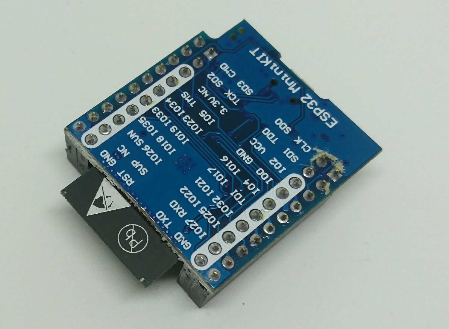
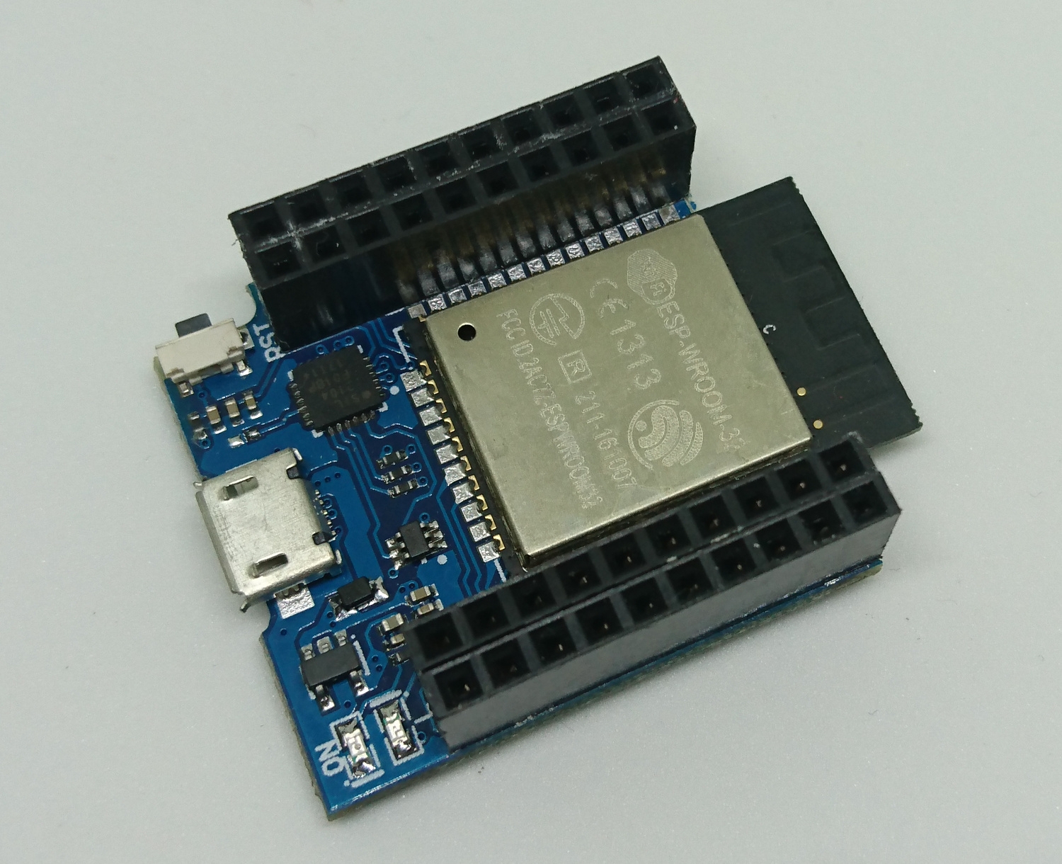
  • ICs like MCUs and various sensor are stored in a grid of small boxes with labels.
  • Boards, china modules, etc. are stored in several paper boxes.
  • All the other components are in plastic bags with a hand-written label. These bags are kept in groups like transistors, diodes, LEDs, etc…

I also think it a good idea to have some parts on stock. I think everyone is familiar with the situation, when you are making a quick fix and you miss the resistor of the proper value. Ordering a component is time consuming (it takes few days to arrive) and costly (there are the shipping costs).

When I design a board I usually draw a schematics with respect to BOM and my home supplies. That means for example, if a value of a resistor is not critical, I try to match it to one of the values I already have in stock. But I do it only based on what I remember as going through the bags is time consuming. This also works only for my current stock, the stock might be different in a year.

I don’t use BOMs with precise order codes as I am a hobbyist, who populates boards manually and make only 1-5 pcs of a board. I have to care about minimal order quantity and I wonder why are there such a big price differences in practically identical components. When I need to order a component, I generate the BOM for several projects and go through the supplier website finding a component to match my needs with respect to price. I also try to match the components between projects. I don’t care much if I receive my components in reel, tape or a bag (precise order code usually forces me to buy a given packing, which can be in low quantities expensive). The process of ordering components is slow and annoying.

Also there is always a problem to decide what to order and what not to order. I usually base my decisions on my poor memory – I often don’t remember exact quantities I have on stock (and I am lazy to go through it). Therefore I rarely miss a component and usually order something I already have on stock. Also sometimes I order components for a project, which is for some reason left unfinished. Therefore my stock is constantly growing and contains components I will never use again (in my current workflow).

To sum it up – it is a little bit messy. From my experience, I am not the only one having this issue. Even some small companies have it.

What Would Make My Life Easier?

All these problems boil down to common source – component specification. When you use a component in a schematics, you should specify it. People use two methods:

  • They supply the part value (resistance, capacity, voltage etc.) and sometimes they add other criteria (e.g. power rating of a resistor).
  • Or they supply precise part name or event an order code for a supplier of their selection.

The second method might work for large companies producing thousands of boards – it is easy to order the components and the designer has everything about the components under control. It is also a good way to go with ICs and special components on hobbyist boards. However, when it comes to passives as resistors, capacitors, coils, etc., it does not work well for the hobbyist. If you specify the order code, then it is hard to use your stock supplies. If you decide to stick with a single type of your resistors or capacitors for the stock, it can get quite pricy, as you cannot buy the cheaper alternative. Also if you decide to build a board designed by someone else, you either have to match you stock supply with the order codes on the board or order components specifically for the board.

Let’s take it to the extremes to illustrate my point; when I have a small toy board, I don’t care whether a pull-up resistor is 10k or 12k. I want to specify it to be in range 8k-15k, in 0603 package and power rating greater than 0.05W. Nothing else, like manufacturer, height of the package doesn’t bother me. And any component fulfilling this specification will work for me. The same with capacitors – I usually need a given capacity, least voltage rating, package and min/max ESR and nothing else (like dielectric material) doesn’t bother me a lot in many cases.

The previous paragraph was rather extreme. Usually what I aim for is to make following step easy and repeatable for different settings: “I need an order code for the cheapest resistor with this value, at least this power ratig and with a tolerance at least 5%”. And ideally make the procedure automated based on schematics and allow for merging of BOMs and their simplification (e.g. I can replace 5% resistors with 1% resistors).

Let’s be honest – I think many hobbyist does exactly the same thing when order components for their designs. They do this matching by hand. And it can be a source of bugs as the specification isn’t written anywhere – especially if you are not the author of the board and you don’t know what parameters are critical. Well, it is usually enough that you order for a board designed a year ago.

Therefore I would like to keep track of this specification in schematics. I would like to attach attributes with the specification in KiCAD; like “resistance > 10k && resistance < 12k", "package ~= (0402|0603)". Then I could use an automated tool, leveraging for example Octopart, to find a part matching my criteria. Of course, if something needs to be precise, I put precise specification for the component.

Having this option would also motivate me to store my components in bags/boxes with a sequential numbers and the precise part name and keep an electronic track of my components. Then I could just export this “smart BOM”, verify it against my database and find out, that I should use 100n capacitors from bag nr. 42 and the remaining two capacitors can be taken from a bag nr. 87 (as they probably differ in voltage rating, but I don’t have enough of the first variant). This would force me to reuse most of my stock material and I would by only the necessary things.

It would also ease the situation when I need to find an alternative for a component as I miss one component and I prefer to buy it from a local seller to save time. But the seller does not have the precise component. Given the specification, I know which parameters of the component are crucial, and which not as much. The same case is the situation when I want to build someone else’s board and use as much stock material, as possible.

The Tools

I am not aware any of any ECAD program out there, which would support such a specification of components. Is there something out there I miss? Even a third party service I am not aware of? Do you see any flaws in the component parameter specification? If so, please let me know!

For me the outcome is: This can be easily added to existing tools like KiCAD and Eagle – both of them support attributes. What is needed is a format of these attributes to specify the constraints. Then we can easily build tools on top of it, which will make our life easier.